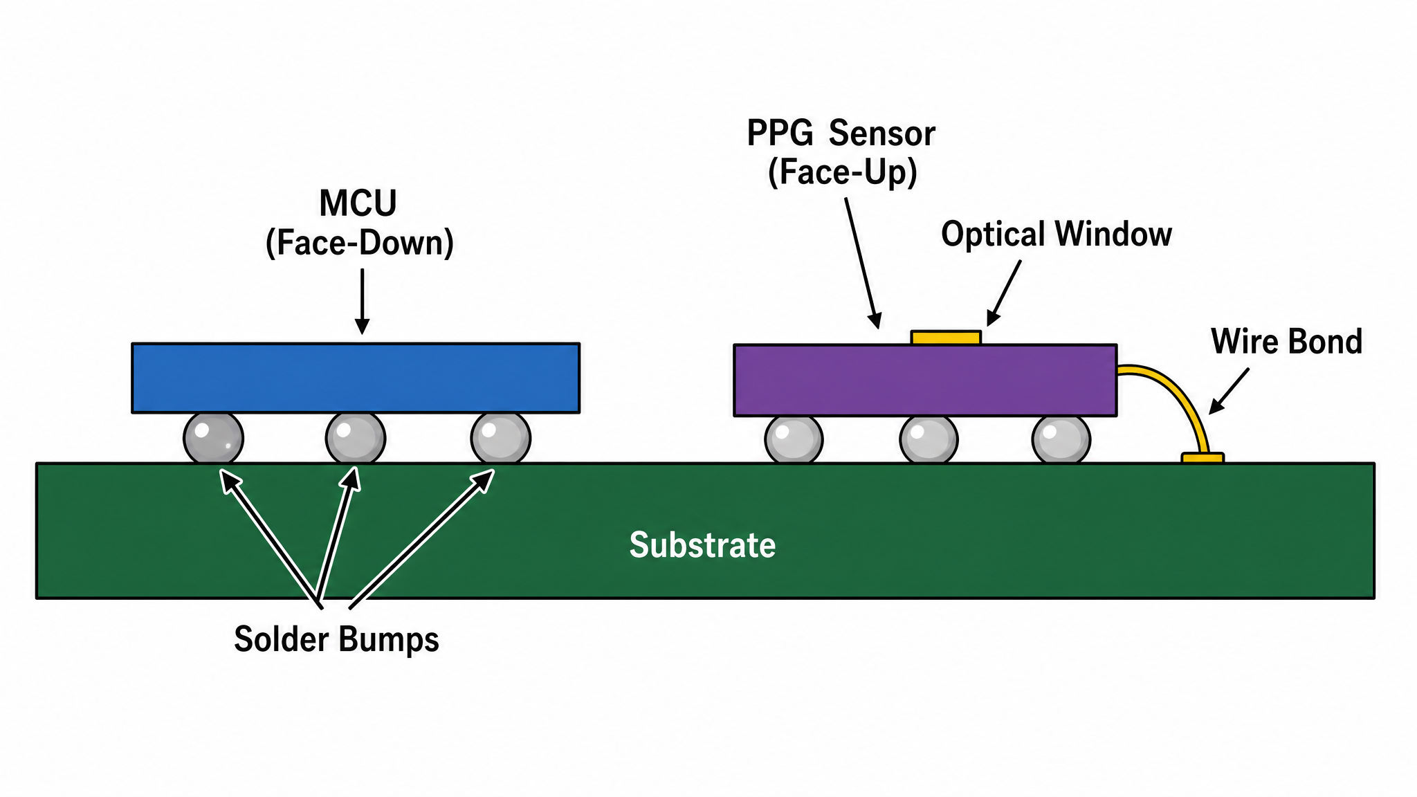
Diagramme de Boîtier de Semiconducteur
créer un diagramme technique avec iagénérateur d'illustrations médicales iagénérer des illustrations avec iagénérateur de diagrammes d'ingénierie ia
Prompt
A clean, minimalist 2D engineering cross-section diagram of a semiconductor package on a white background. At the bottom is a wide dark green rectangle representing the substrate. On the left side, a blue rectangular microchip is mounted face-down, resting on three small, round silver solder bumps. On the right side, a purple rectangular microchip is mounted face-up, featuring a tiny yellow square on its top center. A thin curved wire connects the right side of the purple chip down to the green substrate. Clear, simple text labels pointing to elements: 'MCU (Face-Down)', 'Solder Bumps', 'PPG Sensor (Face-Up)', 'Optical Window', 'Wire Bond'. Flat vector graphic style.
Plus comme ceci